TP4056 PCB Layout in EasyEDA

Now we know how to make custom footprints and assign them to the symbols within the schematic editor in EasyEDA. So it's time to transform our schematic into a fully functional printed circuit board design that is ready for manufacturing.
Wait, why did the heading changed from IP5306 to TP4056 so fast?
TP4056 is one of the most popular charging modules available, so it would be fantastic to create a version 2 of the famous TP4056 charging module. It’s not something new; many have done it before. However, I want to make sure this works as a drop-in replacement for the TP4056 with the exact size and dimension while retaining all features of the IP5306.

EasyEDA: Creating PCB Layouts in EasyEDA
So, let’s start with a common mistake beginners make when using EasyEDA: creating a new PCB layout file directly from the file menu. Although it works, it doesn’t automatically import all components and connections to the PCB editor, making the PCB design messy and challenging to work with. That’s why we build the schematic first and then transfer the connections to our PCB layout.
To do this in EasyEDA, navigate to the schematic editor and select ‘convert schematic to PCB’. This action will create a new PCB layout file in a new tab and prompt you to enter your new PCB’s dimensions.

Here, most options are self-explanatory: set units to mm, number of copper layers to 2, board outline to rectangular, start X and Y to 0 (which positions the PCB outline at the document’s center). Finally, enter your desired width and height for your PCB dimensions. Since we’re creating version 2 of the TP4056 module, we’ll use the TP4056 modules dimensions: 27mm width and 17mm height.
Once the values are entered, hit apply!
You’ll see an outline for your PCB with your specified dimensions and all components and connections from your schematic editor.

Component Placement and Layout Optimization
Now let’s move on to component placement on our PCB. We’ll start with larger components and work our way down to smaller ones. To move a component, click and drag it to your desired location on your PCB. In any case, if you want to change the orientation of the component, just use the shortcut ‘R.’.
Let’s start by positioning the USB C on the left side of the PCB for easy access. If you’re finding placement of the component a little difficult, it could be the grid’s close interval snapping; you can adjust this in the object pane on the left. Let’s set the snap value to 0.5mm.

Now, you’ll notice a difference in how components snap to the PCB, allowing for more precise placement. Alternatively, let’s select a component and directly adjust its X and Y locations in the object pane. For instance, if you enter specific values here to center the USB C symmetrically on the PCB.
Next, let’s bring in the IP5306IC.
Now, let’s bring in the larger components, like the inductor and LEDs. If you’re unsure about their placement order on the PCB, you can always refer back to the schematic that we did for reference.

Next, let’s position the input and output jumpers as precisely as possible to mirror the TP4056 IC. Hmm, it seems we’ve run into a bit of a snag—all components won’t fit within this PCB. We might need to slightly increase the PCB size.
To do this, let’s delete the existing PCB outline and create a new one. Go to ‘tool’, click on ‘Set Board Outline’, and increase both width and height by 1mm (to 28mm and 18mm). Then hit ‘apply’.
Now we can move around the components and adjust them until everything is packed tightly. While doing this, just remember one major point: input pins, USB C, and output pins need to be in specific spots with certain dimensions because we’re replicating the TP4056 module. Use the measure tool as often as possible to double-check distances. And once you are happy with the location, lock the components in place using the lock option in the object pane.
Once these components are placed, bring in the rest of them within this board layout. Make sure you refer back to your circuit often, and try to place components close together to avoid making long tracks when you start the routing process.
It might take a few tries to plan and place components effectively around your PCB. Once satisfied with the layout, we can move on to routing!
EasyEDA: Routing Connections and Using Vias in PCB Design
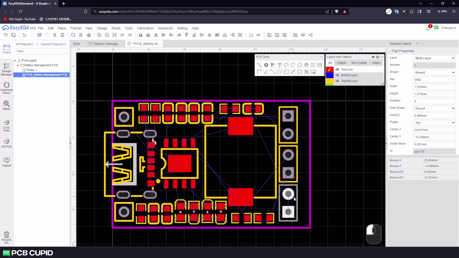
You might notice some connections floating across your PCB; these are called rat lines [shown in the below figure]. They represent connections made in your schematic but not yet established between components on your PCB.

The process of creating these actual connections on your PCB is called Routing. It’s quite simple to do in EasyEDA; all you need are these two tools: the "track" tool and the "via" tool.
To keep the routing process simple, use your schematic diagram as a reference and start routing from one side of your sheet to another and o make the connection, start by selecting your track tool and clicking on a component from which you want to start connecting. Here, let’s start with USB C and an input power circuit for an IC.
Click on a pad where you want to start and another where you want to end to make a connection. But remember, drawing tracks within your PCB isn’t always straightforward, especially when dealing with complex or high-speed circuits. There are many guidelines that you need to follow to make the routing very effective.So to learn more about routing process in detail and also some basic outlines of the PCB design guidelines, click here.
The first track was straightforward to layout, but what happens when there’s no way to connect the tracks on the same layer? In such cases, we need to use the bottom layer of the PCB to create a jumper connection. This is where the via tool comes in handy, creating a small hole to connect the top layer to the bottom and vice versa. Here’s (Near to the usb C) a simple example of how via works on both layers.

Implementing Ground Pour for Enhanced PCB Stability
With basic guidelines in mind, start routing the rest of your connections. Take your time and ensure the route tracks accurately with proper spacing and thickness, as discussed in the design guideline article.
You might notice some extra space on the length since we increased it by 1mm. You can adjust this by slowly moving the outline points inward. This should bring us back on track with a size similar to TP4056 but slightly larger in width. But that shouldn’t be an issue as long as we maintain the correct distance for pinouts like the TP4056 module.
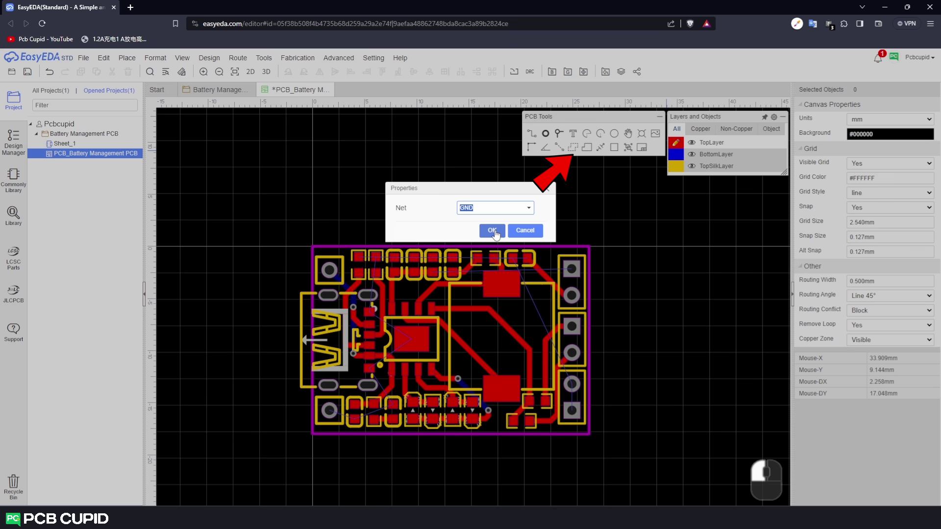
All the ground tracks are left out because you are going to do a ground pour. This will connect all ground connections together in a larger copper area. While you can complete the circuit just with tracks, a ground pour offers many advantages: it’s easier to etch during PCB manufacturing, can act as a heat sink, provides overall circuit stability, and reduces EMI.
To create a ground pour, select the copper pour tool and set the copper pour net name to ‘ground’. To do the pour, start drawing a polygon around the PCB by clicking at all four corners. Once you complete the polygon, just do a right click, and you’ll see how some of your ground rat net connections disappear. So, let’s repeat this process for the bottom layer as well.
Finalizing PCB Design with Text and Logo Addition in EasyEDA
This technique should suffice for most modern manufacturers with this default clearance value. However, Its recommended to cross-check the value with your PCB manufacturer before proceeding. As a safety measure, slightly increase the clearance value so that you can send this for manufacturing with a wide range of manufacturers.
If you notice any missing connections (like this ground not passing through this small space), you can fix it by adding via to both top and bottom copper pours.
If you look closely at the TP4056 PCB, you’ll see several vias on the bottom. These are called stitching vias and are essential in many circuits for transferring heat from components to the PCB for thermal stability.

So, let’s return to our PCB editor and quickly add this pattern to our circuit using the via tool.
With this, we complete our electrical connection.
Usually the names are on the silk layer for easier assembly, but since our PCB is compact with little space on top, let’s add text on the bottom layer along with a logo.
To do this, select the bottom layer on your PCB and use the text tool. Place it where you want it and adjust its layer, content, font, and size in your object pane.
Let’s finish the PCB by adding a logo as well.

To add a logo to your PCB, use the image tool in the PCB tools panel. In the pop-up, select your preferred logo. Adjust the image settings until your logo is a perfect black-and-white image suitable for use on your PCB. Finally, set the dimensions of your logo to fit your PCB design.
Once you’re satisfied with all the settings, place the component where you want it and click your mouse’s left button.
This wraps up our PCB design using EasyEDA.

Viewing and Preparing PCB Designs in EasyEDA
If you’d like to see a quick 2D image of the PCB without layer clutter, simply click on the 2D icon in the toolbar.
Similarly, if you’d like to view your PCB in 3D format, click on the 3D icon. This will display a stunning 3D model, complete with all the components used on your PCB.
Currently, let’s hold on until manufacturing the PCB because we should even discuss more about DRC and gerber generation and learn how to create custom panels in EasyEDA for cost-effective and error-free production.

Also, you can watch the complete video tutorial here:
This brings us to the end of the article. In the next article, we will discuss more about How to Perform DRC & Gerber Generation, until then keep learning and keep creating!
If you have any queries, please drop them here