Introduction to KiCad

It's been a few years since KiCad version 6.0 was launched and KiCad has already launched their version 7.0 (subsequently version 8.0). KiCad comes with great new upgrades like orthogonal dragging, drag and drop, command line interface, text box support, schematic and symbol editor, etc. which were not in 6.0. Read more about KiCad release in news.
As of Feb 23,2024 kicad.org launched KiCad 8.0, but this tutorial should be helpful even though it was made for KiCad 7.0 as there were only few minor upgrades on UI and functionality over version 7!
What this article talks about
This article is an introduction and first among the “KiCad tutorial” series. In this first article, we’ll cover downloading and installing KiCad and quick walk-through the features of KiCad.
Also you can watch the complete video Tutorial here :
Introduction to KiCad itself!
For those of you unaware of what KiCad is, let’s go through it quickly. KiCad is an open-source software for creating electronic circuit schematics, printed circuit boards. Along with they also offer:
- PCB calculator for determining electrical properties
- Gerber viewer for inspecting manufacturing files
- 3D viewer for visualizing the finished PCB
- Integrated SPICE simulator for inspecting circuit behavior.
If you are unaware of these feature, worry not! We’ll make sure we discuss everything in detail through this KiCad series.
Downloading and Installing KiCad
Here’s a simple 4 steps process to download and install KiCad:
- Go to KiCad.org
- Click on ‘Download ‘ button that’s right in the middle of home page
- Select the operating System of your machine
- Click on GitHub
Once you have downloaded it’s a straightforward process to install. Follow along the installation setup window to finish up the process.

This step might change depending on the type of operating system you use.
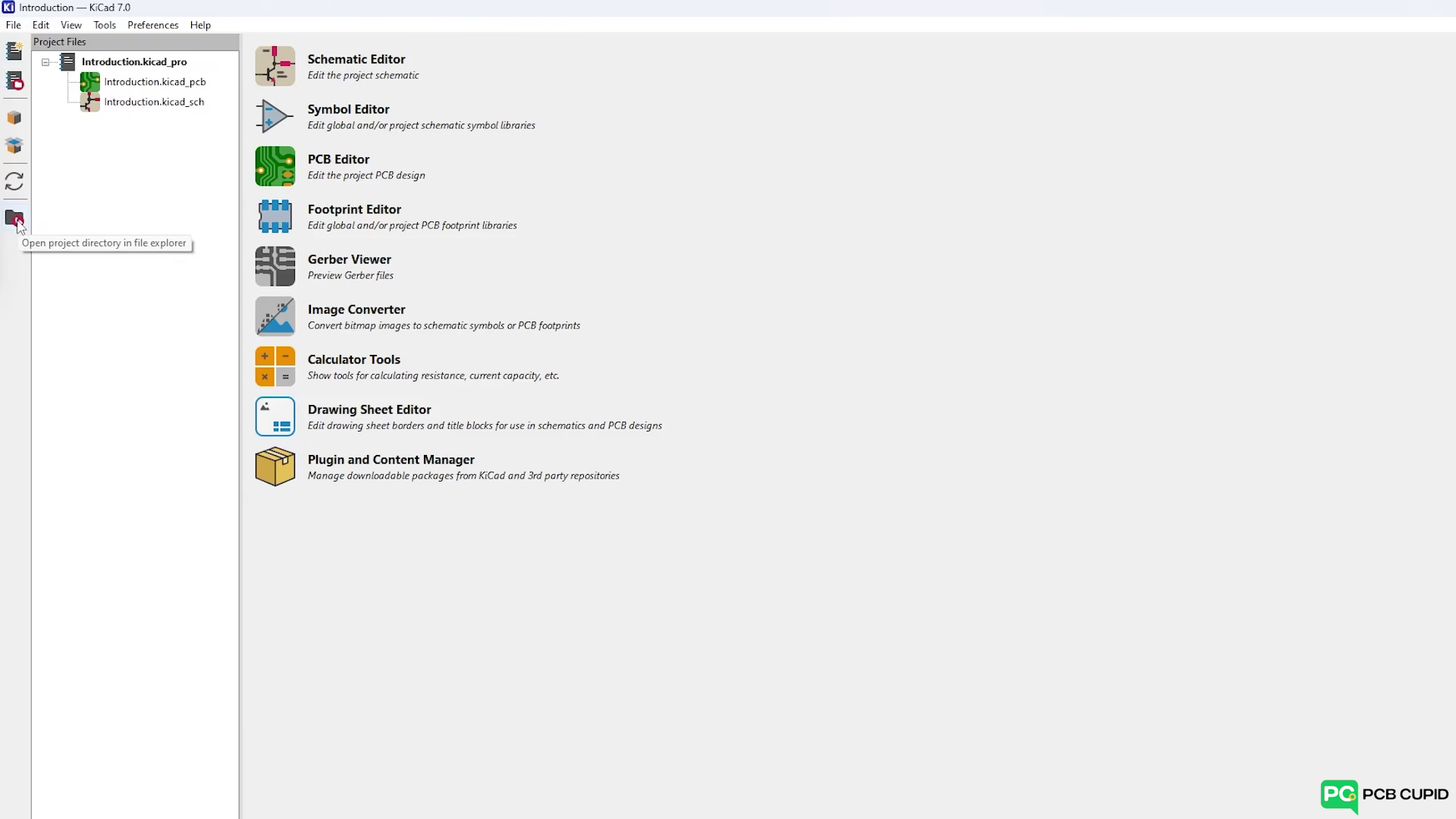
Now you can open the Kicad and this is your project window which shows all the files that’s related to the project (also shown in the photo below).

To have a better understanding let’s start with creating a simple project. Either click on file and then create the project or click on the ‘Create new project’ icon to create a new project. In the pop up window, name the project. Let’s name it “Introduction”. Now, there should be two files that created. The first file opens PCB layout editor which helps in making traces and arranging of the components. And the second file opens the schematic editor which helps in building the circuit with electric symbols.
To see where the files are locally stored in your system’s memory, click on the “Open project directory in file explorer” option at the bottom left bar. That should redirect you to the folder where the files are locally stored.
Features
Schematic Editor
This is where the PCB journey starts by creating electrical connection between the components and how they work together. This is just purely for representation and this won't include the physical data of the component.

Symbol Editor
KiCad comes with some standard symbols but often there are situations where some symbols (that we need) are not available by default. So KiCad gives an option to build and customize symbols ourselves.

PCB Editor
This is where the electrical connection done in the schematic editor gets converted into real world PCB along with measurement of the components; how they are arranged and how they are physically connected.

Footprint Editor
Just like the Symbol only some standard Footprints are available in KiCad by default. In such case footprint editor can be used to make custom footprints.

Gerber Viewer
Gerber is the output file that should be sent to fabrication plant to manufacture a PCB. So, the Gerber viewer option enables to view the file before sending to the manufacturer.

Image Converter
This tool is used to convert images like JPG, PNG into formats that KiCad can understand and place it on the PCB. This process can be used to place logos, images and instructions on the PCB.

Calculator Tools
This tool can be used to colour code the value of the resistor, calculate the track width via size, electrical spacing, etc.

Drawing Sheet Editor
This tool will help in customizing the schematic editor sheet like adding names, logos and other details which are very helpful in case the design is being shared online or within an organization.

Plugin and Content Manager
This will help getting 3rd party features in KiCad which are made by community members. More on this in a later article.
The above discussed tools can be accessed through the top menu bar under tools section as shown below.

This brings us to the end of the introductory article on KiCad. The next article will discuss in detail about how the user interface inside KiCad works. Until then keep learning and keep creating!
If you have any queries, please drop them here