PCB STACKUP in KiCad

Let’s start with quickly discussing what a PCB is composed of and how we can relate them in KiCad while using the PCB editor.
Printed Circuit Boards are made of various layers stacked upon each other :
Base / Substrate
First, we have the base or substrate. It’s a fiberglass material, which is the solid core that gives the PCB its rigidity and thickness. It mechanically holds the connections and the components, just like a regular perboard or a breadboard.

Conducting Layer
Then we have the conducting layer. In most cases, this conducting layer is made of copper and connects the electrical connection between the components just like traditional wires. These connections are called traces, and they can be of various widths and lengths depending on what we are planning to connect, which we’ll discuss in more detail as we make our own design.

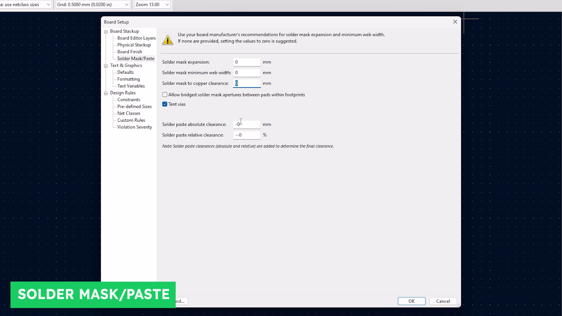
Solder Mask
In a single layer, double layer, or multilayer PCB, it generally refers to the amount of conduction layer in the PCB. We can actually stop at this stage, because we have a usable PCB and it does its function. But when we notice the PCB that we come across in our daily lives, it’s a little different. They come in a green layer on top and this is called the Solder Mask.

It protects the PCB surface and insulates the copper circuit from oxidation. It also prevents accidental contact with other metal, solder, or conductive bits. It can be of any color, but mostly it’s green because it’s easy on the eye and also shows the different traces, planes, and empty spaces.

However, the solder mask doesn’t cover up everything on the board. It’s applied in such a way that it covers up the small traces, empty spaces but exposes some space around the component pads so they can be soldered later.
Silk Layer
Finally, we have the silk layer. This is the layer at the top with the name, letters, and symbols, and is usually white in color. It just makes the assembly and finally working of the PCB convenient.

Navigating and Configuring KiCad PCB Layout Editor Layers
Now lets see pcb layout editor, so go to schematics and click on pcb in board editor. The editor is pretty simple to use, and it uses the same buttons and navigation style as the schematic editor.

For the board stackup let’s start with setting up the board. To do that, click on the board setup icon.
Below it select the board editor layers.

Here, the prefix ‘F’ stands for front, and the prefix ‘B’ stands for back. Based on this, we have the front and back courtyards, which define a safe area around a component so that while assembling the physical components, they don’t overlap each other. Then we have the F.fab and B.fab, where we can give more data to manufacturing without including them in our board, like mentioning some import points or notes. For now, let’s turn it off.
Then we have the F.Adhesive and B.Adhesive layers; this layer would be required only if the component is not easy to mount and requires any additional glue. This layer would indicate where the glue or adhesive has to be applied. Let’s turn it off as well, as our circuit won’t need it.
F.paste and B.paste would have information about where we shouldn’t apply the solder mask so we can solder components. Also, these layers are essential in making stencils.
Finally, there is the edgecut layer, which will define the PCB shape and dimension.Also, We can use the margin layer to define the area where the component’s, traces and any other parts of the PCB are allowed to be placed or not allowed to be placed.
Hmm, seem's like there's are lots of layers than we discussed, but we won’t need most of them. So let’s turn off the things that aren’t required.
Let’s turn off UserEco; this layer is used only if you are sharing the PCB layout file with other engineers. Here, you can include revision graphics and drawings that won’t be in the final product. We can also turn off the drawing and comments, which are generally used for user reference and have little to do with the PCB. Finally, we can also turn off users; they are user-defined layers where we can add special features to the PCB and also convey them to the fabrication plant.
Managing PCB Layers and Settings
Next, we have the physical stackup; this is where we assign the number of layers. In our case, we’ll be using just 1 layer to make our PCB. So we don’t have to mess with the rest of the settings; most of these values will be taken care of by the fabrication plant.

Configuring PCB Surface Finish and Appearance Settings
Then we have the board finish; this will tell you how you need the surface finish of the PCB.
In these settings, we can either use the information from the manufacturer website or fill it in, but in most cases, there are good results with just default values. So let’s just leave it as it is.

Next, the Text & Graphics, These settings are just for appearances, and they don’t affect the PCB in any way. You can change the line thickness, text, and other information.
This brings us to the end of the article, you can watch the complete video tutorial here:
Next, we’ll add some design, bring all the footprints, and start with laying out the PCB. Until then keep learning and keep creating!
If you have any queries, please drop them here