Footprint Assignment Tool in KiCAD

In the last aritcle, we discussed various factors on how to select the right footprint for your components. Now, we’ll discuss how we can assign the footprint to the components using the KiCad’s footprint assignment tool.
Footprint Assignment Tool

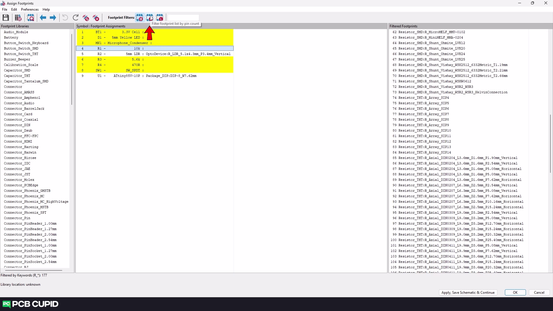
Here we can see some of the components are assigned by KiCAD and unsigned components are highlighted in yellow (shown in the figure above). This window is primarily used to assign the correct components to the symbols, to understand how this tool works, let’s start with the menu bar.

The second option on the menu bar takes us to the footprint libraries. Where we can see all the footprint that’s available on KiCAD and it’s physically location that’s stored on the computer. We can also use this same option to include custom libraries or external libraries that’s created by community members.

Then we have, view the selected footprint. This will open the footprint and show it on a different window. You can either use this button or you can click on the component to select the component and then a right click and finally click on the view selected footprint, as shown in the figure below.

Footprint Viewer
This opens a footprint window, which is fairly easy to use. Where most of the tools and navigation are similar to the schematic editor. You can zoom in, zoom out and pan same control as before and also use the tools on the top and left toolbar as we discussed in the earlier article.

The primary purpose of this window is to confirm the correct footprint that we’ll be using in the project. Here, we’ll be majorly using the measure tool (shown below) to measure the component dimension and check for compatibility with the physical component.

The below outline tools also can come in handy to hide unwanted details on the footprint, for example the hide/unhide pin tool:

Outline mode for pads:

Outline mode for texts:

And outline mode for all the graphics:

Unfortunately, this window is to just view the footprint and we have no way to edit or modify. In future article we’ll look into how to customize and edit the footprint using footprint editor. For now let’s continue with the footprint assignment tool.
Assignment Tool Menu Bar
To go through all the unassigned components you can use these two buttons to navigate and find the unassigned component. You might already what the next two buttons (undo and redo) so we’ll skip them and go to the next option.

This option is little tricky and can make you think KiCAD would assign all the components with some default footprint with just a click of a button. But that’s not the case, KiCAD uses a special footprint association file to assign footprint to the component and this file has to be manually created.

To add the footprint association file you can go under Preference -> Mange footprint assignment . In this pop up you can add the footprint association file.

Let us give you a gist of how this footprint association file works with an example. So, let’s assume we have some collection of components that are already procured. Based on which we can create a footprint association file with the format that KiCAD is looking for and when that is done, we can include this footprint association file while doing any project that we’ll use the same procured components and it will automatically assign the footprint to the components that we already have.

This might seem a lot of work, but when you are working as company or giving a service to multiple client this can reduce a ton of work down the road. So far we explained this about the footprint association file just for information and it’s not something we would recommend for beginners or who is just getting started with KiCAD.
Next option on the menu bar is pretty simple. This will reset all the footprint associated to the symbols.

Narrow down to 1 Footprint!
If notice at the bottom status bar, you can see we have over 12,000 footprint that are by default installed with KiCad. There are times this can slow down your computer when you search for a component. To solve this, KiCad has some custom filters that we can apply during search and narrow down that one footprint that’s you actually need.

First we have a filter footprint based on the symbol description .

This will just show us all the footprint that is related to the symbol. In this case we can show all the components that are related to resistors and we have brought down our option from 12000 to just 177 footprints!
To reduce further we have the pin number filter.
For a fact we know that our resistors have two pins, but some of the footprints here have more than two pins, so we’ll remove the footprints that have more than two pins by selecting the pin filter, KiCad has narrowed down the footprints to 136.

But it does show footprints from various libraries, like THT and SMD. In our case we’ll be using THT so, to filter by THT use the next filter ‘filter by library’. Turn ON the filter and just click on the footprint library where we need to search, that would be the resistor THT.

Now we have narrowed down from 12k footprints to just 88 footprints. That’s amazing!! We are now just left with narrowing down to the one footprint that we need.
In our collection, we have the resistor of the length 6.3 mm and the diameter of 2.16mm.


KiCad Naming Convention
Now how do we find this footprint in KiCAD? Let’s break down the names that are available for us in KiCAD.

First we have the package name, resistor THT, followed by DIN code, a standard used to differentiate the various types of resistors that’s available in the market. Then we have the ‘L’ which tells us the Length, ‘D’ which tells us the diameter, ‘P’ stands for pitch which tells us the distance between the leads, and finally we have orientation which can be vertical or horizontal.
We would choose the below footprint which has the following features: horizontal orientation, it’s just easier to solder as well as easy to place and we don’t have to fold the resistor which is the case with vertical orientation. If we measure the length and width, it is approximately the same. Then there are also other reasons which are based on design constraint or assembly constraint which you will deal differently for each project.

Assigning The Footprint
Before adding the footprint to the symbol we can double check by cross verifying measurement and viewing it on 3d.
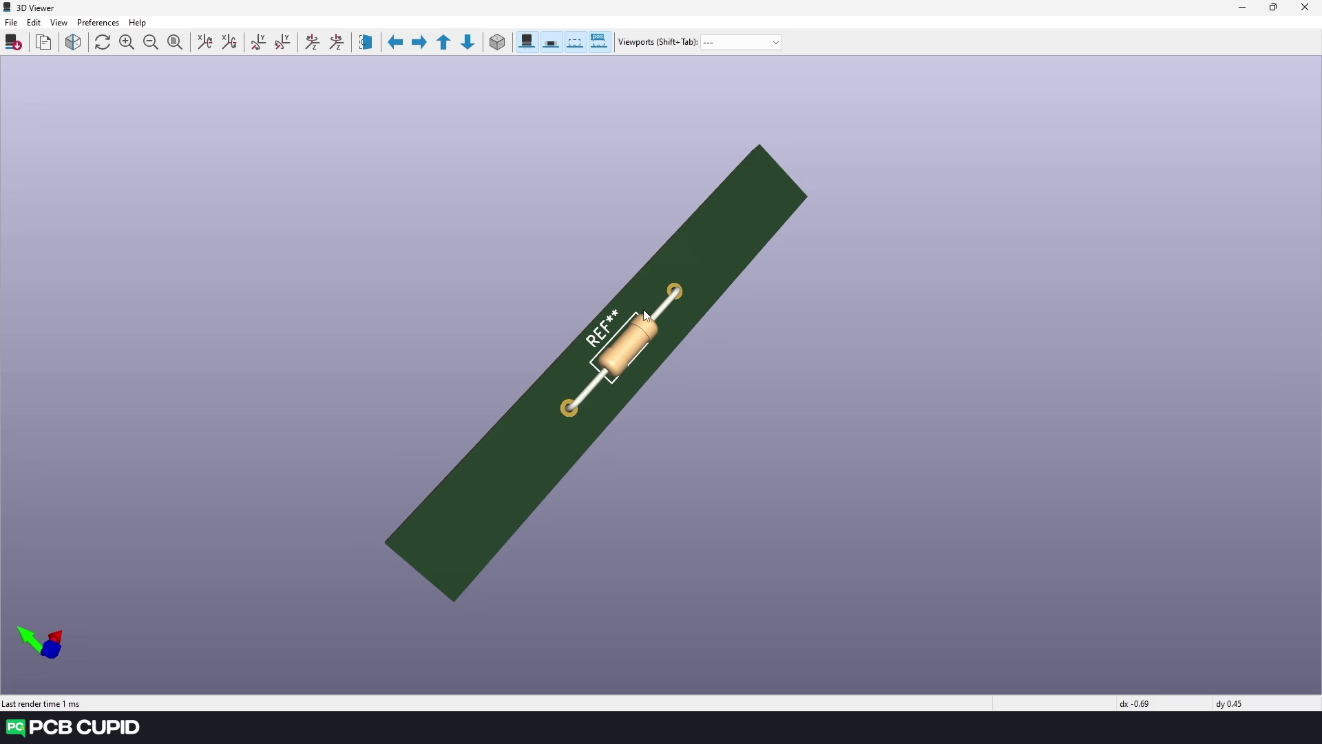
Don’t worry much about the tools and navigation on the 3d viewer. We’ll have a dedicated article for that, but for now just remember to right click move to rotate the PCB, middle click move to pan and finally you can zoom-in/zoom-out with the scroll wheel.
To assign this footprint to the component, exit the view window and go to footprint assignment window and select the component and then double click on the footprint that needs to be assigned to the symbol. You can follow this procedure to assign footprint to rest of the resistors and other components.

The tricky part in footprint is when we don’t have a footprint. For example in this particular circuit the condenser microphone footprint isn’t available by default in kiCad. In this case we would either download a custom footprint or make our own footprint using footprint editor . But we never discussed these, so we’ll try to find another symbol with similar shape/dimension and replace it for now. So, we are placing this footprint temporarily instead of the microphone, as they both look very similar and take the same space.

After assigning footprint to all the symbols, click on* ‘Apply, Save schematic & Continue* ‘. After that click on ‘Ok’
Once all the components assigned, let’s see how all the components look together on a PCB using 3D viewer.

This completes the footprint assignment article. If you like to watch a complete tutorial as video please check this out:
In the next article we’ll see how we can put all these together on a PCB. So far, if you have any doubts or questions, you can always reach out to us at using PCB Cupid Q&A.
Until next article, keep learning and keep creating!