PCB Layout editor in KiCad

From the previous article you should be familiar with Constraints and Net Class Directive tool. So, in this article we'll fully focus on designing the PCB using this editor.
Here, first make sure the edge-cut layer is selected and select the circle tool. And then draw a circle of any radius.

Then press Esc to come out of the circle tool. Now click the circle and press the keyboard shortcut E, or use right-click and click on properties.But I will go with the easiest option by clicking the keyboard shortcut ‘E’.
Using these properties, we can change the location of the circle on the document, and by using these properties, we can change how the circle looks on the document. For now, let’s just set the radius to 30mm.

And also, check the locked option. This will make sure we don’t accidentally move or resize the edge layer. We can see that once its applied to the properties, we don’t have access to the circle anymore, and we won’t be able to select the circle for modification. But if you want to apply some changes to this shape, we can go to the bottom right corner and under the selection filter, check the locked items and that should let you make the modification to the circle even when it's locked.

Verifying Shape
This section filters; we’ll help in selecting only the required items, and it will prevent users from selecting unwanted features of the PCB. In this case, let’s make sure to turn off the locked selection. It’s not mandatory, but this will prevent us from accidentally changing the locked values.

Now, going back to the PCB, we can quickly verify that we have defined the shape of the PCB on the 3D viewer by using the shortcut ALT+3. The 3D viewer output will be this only if the shape is on an edge-cut layer; if the shape is drawn on another layer, Kicad will try to automatically draw the edge-cut layer based on the content we put on the document.

Import from Schematic
Since we have the base ready, all we need to do is get the components and place them within this circle. It should be pretty easy, as we converted all our symbols into footprint in the previous article
On the top toolbar, click on the update PCB button. This will help in importing all the symbols with footprints into the PCB editor. Here we can keep all 3 options checked, and if you like to know what each one of them does, you can just hover the cursor over them, and they’ll have pretty good explanations.
Now click on update PCB and then hit close.

Component Placement in KiCad PCB Editor
We can see the complete circuit is imported and moves along with the cursor. So let’s bring the cursor close to the circle and try to place it within it.

The circuit is a little chaotic and not properly arranged. We need to arrange components in such a way it’s easy to fit on the 3d design. You can download the 3d model for reference from the link in the description.
Here you would be already familiar with most of the tools, they are similar to the schematic editor tools that we learnt in the previous articles. So, here we won’t go into much in detail how things work.
Take look at the reference image above to see how we can place the microphone then followed by LDR and finally the LED. We won’t have control over these placements of these 3 components because of the features we need. But we can move other parts around and optimize the space occupied on the PCB.
Ratlines in KiCad
If you notice there are some lines going across the components; these are called ratlines. They correspond to how the components are connected in the schematic diagram. If it’s annoying, we can turn it on or off using the button on the left tool bar, and you can toggle the button to change the way the rat lines are drawn.
Sometimes these lines can be very confusing if you have way too many components. In that case we can turn off all the rat lines and use this tool.

Component Placement
Do reduce the routing distance place the components close to each other based on the connection (during this you can turn on / off the ratlines).
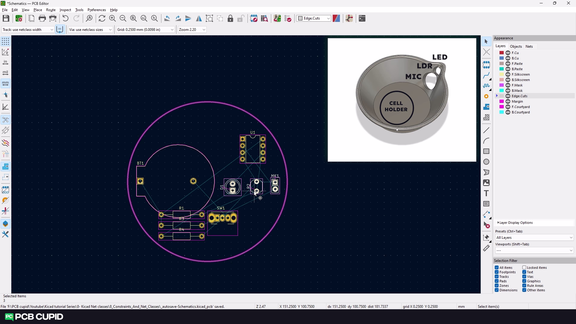
Here we tried to keep all the components as close to each other as possible and also a little packed together. So we can use the rest of the space for adding logos and other information.

Overall, this looks pretty good. We can quickly fix this by selecting these resistors and right-clicking. Click on align, and then align to the bottom. I will do this again, but this time I will click on distribute. This will make sure the components have enough space. I will use this technique to align the rest of the components.

Now it looks way better!
We can quickly check how it looks in 3D by using the 3D viewer (shortcut : ALT + 3).

Integrating External 3D Models into KiCad PCB Editor
Hmm.. the PCB looks good, but it looks very odd with this pin for MIC and no 3D model on the other component. So let me show you how we can quickly add external 3D models to the PCB layout editor.
You can either create your own 3D model or go to the website like GrabCAD to search for the components you need.
Once you make your custom 3D model make sure to export them in .stp or .step file (it's the same if you download the from GrabCAD). With that you can go back to the Kicad PCB editor and go to the properties of the footprint where you would like to add the 3D file and add them here.

For better understanding please watch the complete video tutorial here:
This brings us to the end of the article, until the next one keep learning and keep creating!
If you have any queries, please drop them here