Constraints and Net Class Directive tool in KiCAD

In our previous article we talked about PCB stack up and how we can manage this PCB stack on KiCad. In this article, we’ll start by adding some design constraints and assigning net classes to the PCB layout editor, so we don’t design something that’s very expensive or very difficult to manufacture in a fabrication plant.
Constraints
Pick up from where we left last time and follow along!

Go to the board setup and then select constraints. Here, we need to fill in the values that a fabrication plant can handle. So, anytime we go above this threshold value, KiCAD will warn us and try to keep our design within the manufacturing limit. Usually, all fabrication plants will provide a capability list, which we can use to fill in this data.
If one is just getting started and not sure which fabrication plant to choose, we have a whole section of articles dedicated to that, talking about various fabrication plants, their capabilities and how to place an order with them. Find them here. For now, we will use this capability list because most of the manufacturers can handle these values very easily.
In KiCAD, we have some default constraints; let us quickly see what and why we have these constraints using some examples.
Minimum Clearance

First, we have Minimum Clearance, which is the minimum distance between two tracks. When we go less than the threshold value, we might see some weird artifact or shorting of track during manufacturing. This is because of the process called ‘etching’ that is done during production. To avoid this, we can always design the board a little above the fabrication-capable value to be on the safer side. When we look at the capability list, we can see the minimum is 0.1mm, but 0.15mm is a good value and also recommended by the fabrication plant itself. So, let’s go with that for now.
Minimum Track Width
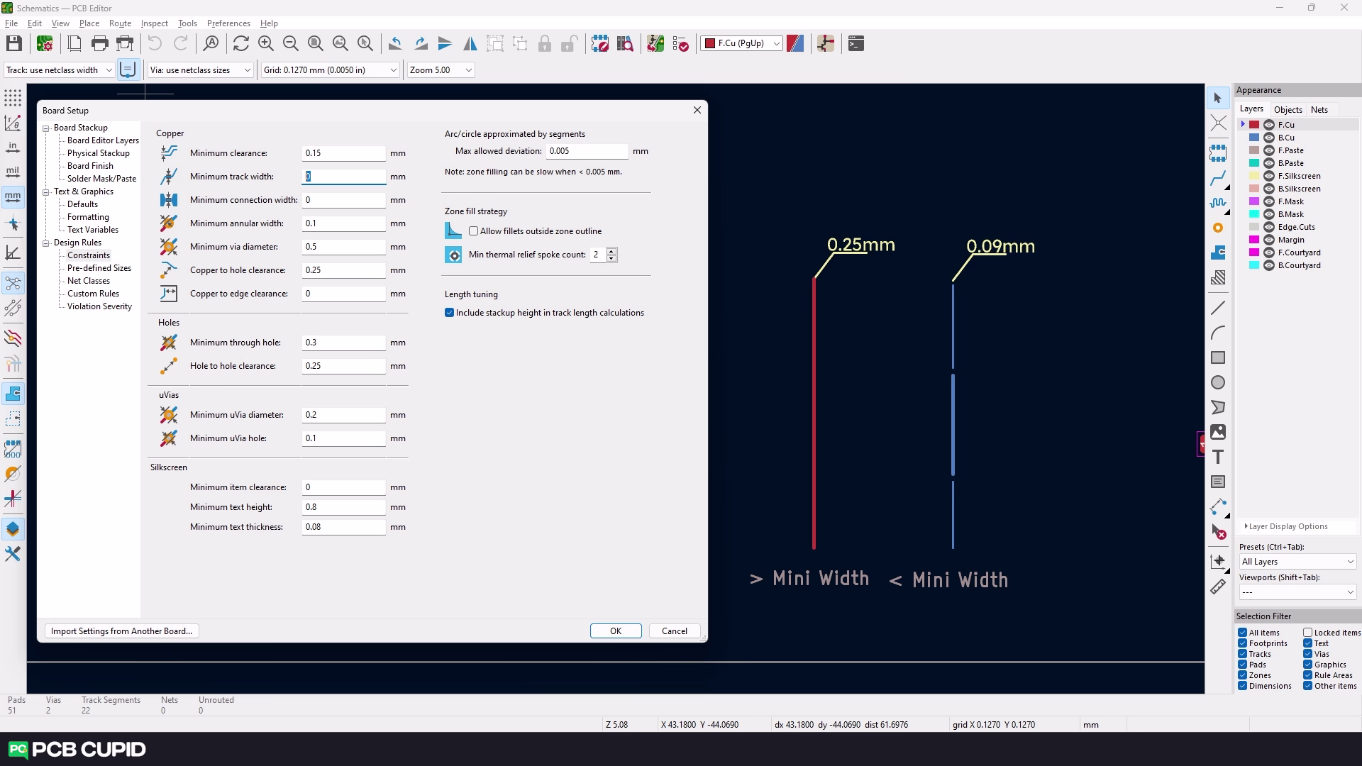
Then we have a minimum track width , which is basically the thickness of the track. Similar to the previous value, this track width is greatly affected by the etching process. If it’s anything below the threshold value, the tracks might cause open circuits in the PCB. According to the capabilities list, it is 0.15 mm.
Minimum Connection Width

Then we have Minimum Connection Width, which is similar to track width, but this is the connection between two components or the connection between a component and track. Similar to the track width, if the value is less than the threshold value, the etching process might break the connection. So we’ll enter a similar value.
Minimum Hole Size

Then we have the minimum hole size; in this case, it’s 0.3mm. We can go below this value, but it would make the PCB very expensive as they would have to use a different process to make the hole instead of using a drill bit.
Minimum Via Size & Annular Width
Next, we have a Via Size of 0.5mm and an Annular Clearance of 0.1mm. To know what these terms mean, check out this cheat sheet of all the terminologies on a single page, which you can always refer to when you don’t understand the terminologies.
Minimum Track Distance & Track Distance Between The Edge Of The PCB

There are two more clearance values: ‘Minimum Track Distance’ and ‘Minimum Track Distance between the edge of the PCB’. The first value will help in making sure we don’t take tracks too close to the holes, which prevents them from being damaged while drilling, and similarly, the second value will help in making sure we don’t take tracks too close to the edge of the board, which might be damaged or chipped off during the final stage of production, where the individual boards are cut off from a panel.
Hole-To-Hole Clearance
The ‘hole to hole clearance’ talks about the distance between two holes. If the distance is not sufficient, then the two very close holes might get fused during drilling and form a single slot.
Micro Vias
Then we have ‘Micro Vias ‘, which are super tiny vias drilled using a precise laser, which can be very expensive depending on the number of PCB products. So this topic can be a little advanced and not necessary for the simple circuit that we are working on. So we can skip to the next section, ‘Silk Screen’.
Silk Screen Clearance
Here, most of the terms are self-explanatory. Like Minimum Item Clearance, it is the distance between two different silkscreen items (ex: a logo and a text). Then Minimum Text Height defined the minimum height for any chosen font, and finally Minimum Text Thickness defined the stroke thickness of the font. I have added all this value based on the capability list from the manufacturer.

Length Tuning
The ‘Length Tuning’ is used to control the timing and impendence of a trace. By using length tuning we can precisely adjust the data transmission time and also power loss on the trace.
Pre-defined Sizes

Let’s predefine some track width that we can use in the circuit; it’s very similar to how we chose a wire to make the connection based on the current rating of the circuit.
For the circuit we are working on, we’ll need two sizes, one for the signal and the other for the power tracks. To calculate this length, let’s open the calculator in KiCad.
Track Width Calculation
Go to KiCAD’s project window and click on ‘Calculator Tools.’

Then select the track width. If you want to know how the calculation is done, you can refer to the formula and the reading section, which have an explanation of how track width is calculated. Since our circuit is simple, we can just enter the maximum current it would carry during operation. I will just enter 1A for now. I know the circuit we built in previous videos won’t even be close to 0.5A, but decreasing the current consumption will decrease the track width, which will make the track width less than our clearance value that we set a while ago.

Then, for the temperature rise and trace length , we can just let them be defaults. As our circuit is pretty small and simple, these factors won’t affect the circuit much. With this information, we have a** track width** of 0.3mm, which we’ll include in the pre-defined track width. If you’re wondering about the track thickness , it’s a parameter that we’ll use to inform the fabrication plant how thick the copper coating will be when we send it for production.
There is something called Internal Layer Traces ; these we’ll consider for the track width when tracks are buried between layers in a multilayer PCB, so this won’t be of much help now. Now with this information, I will create a 0.3 mm track width for the signal, and additionally, I will create a 0.5mm track width for the power. I’m doing this just to show the difference between power and signal tracks, but theoretically, 0.3mm would be good for signal and power.
Net Classes
If you remember from our video about schematics and adding net labels, we discussed how we could name a few connections for easier understanding. Similarly, we can use Net classes and create a group of connections that share the same properties.
For example, we can create two classes called signal and power, which can be used to automatically assign the thickness of the traces to these two groups of classes.

Here, we have just created the classes but never really assigned them to the connections that we made in the schematics. We can do this in two ways.
We can either do the assignment here on board setup or we can do the same on the schematic setup. Personally I would prefer using the schematic setup.
So let me close this and open the schematics editor.
If you click on this connection and see the bottom status bar, you can see that we have the connection name but the netclass is set to default.

To assign this particular connection to signal net class, we can just right click on the connection and select assign netclass. This is just the net label that we assigned and here we can set the net class on the drop down list. I will change this to signal.
We can either do this process for all the connections or we can just go to the schematic setup.
Here we can just enter the name of the connection and kicad will automatically assign the net classes for these labels.
There is a slight problem here. We have assigned net classes only to the connections that have names but what about the ones that’s unlabeled? There is no way to search for a pattern without a name so how about we manually try to assign?
Seems like we can’t assign the net to this connection without adding a net label. We can fix this quickly by adding a net label, but this would become very difficult when we have many connections without the net label. In Kicad we can solve this by using net class derivation to assign net classes to unlabelled connections.
You can click on this icon here and then click on the connection where we want to assign the net class. On this menu select the signal that we need and how they appear on the schematics. Then click okay and place it on the connection.

Now when we click back on the connection, we can see on the status bar that net class has been assigned to the connection.
Now let me quickly assign the rest of the connection with the net class using this tool.
To just make sure the schematic editor is reflecting all the changes to the PCB editor, we can open the PCB editor and then open the board setup to verify.
You can watch the complete youtube tutorial here:
I know this is a lot of work for such a simple circuit, But you need to trust the process, these settings will really help a lot in making a very good PCB at the first try. But during this journey please try to use forum for the questions you have, it will really help us in producing more videos also it will help many people users who are just getting started!