Creating Custom Footprints in KiCad
 There are quite a few times where KiCad’s default footprint won’t be sufficient for the project. In this case, we are either forced to create our own footprint or try to find a footprint online for the component that we are working with.
now we’ll see both methods, where initially we’ll create the footprint using the footprint editor, then add an external footprint that we found online.
In our PCB, there are quite a few things that need to be optimized.

Look at the cell holder footprint, for example. The 3D model is way smaller than the actual footprint. That’s because we used a different-size cell holder as an alternative instead of using the actual footprint. This can happen quite a few times because Kicad cannot hold all the footprints that are available on the market.
Now, let’s try to fix this by making our own custom footprint.
We can’t just dive in like the symbol editor; to make the custom footprint, we need to have proper details about the component, like the shape and its dimension. Because the footprints will reflect the actual physical.

Luckily, we could find the datasheet for the cell holder, which has a very precise measurement.
Creating Footprints for Cell Holder in KiCad
With the datasheet, we can jump into the footprint editor to create the footprint for the cell holder.
You can either click on the footprint editor icon from the PCB editor or directly access it from the KICAD project window. This footprint editor has tools and navigation systems that are very similar to those in the Kicads PCB editor. Except we have all the footprints available on Kicad, arranged here alphabetically.
To start, we’ll create a new library just like we did for the symbol, so this way we don’t mess up the default ones.
Go to File and click on the new library.

Now, while naming, let’s use Kicad’s library convention, so the name of the library will be something like “CellHolder_THT.” . This is not mandatory, but trust me, it helps a lot while managing a huge number of custom libraries.
Once the library is created, select the library and then click on “create a new footprint”.
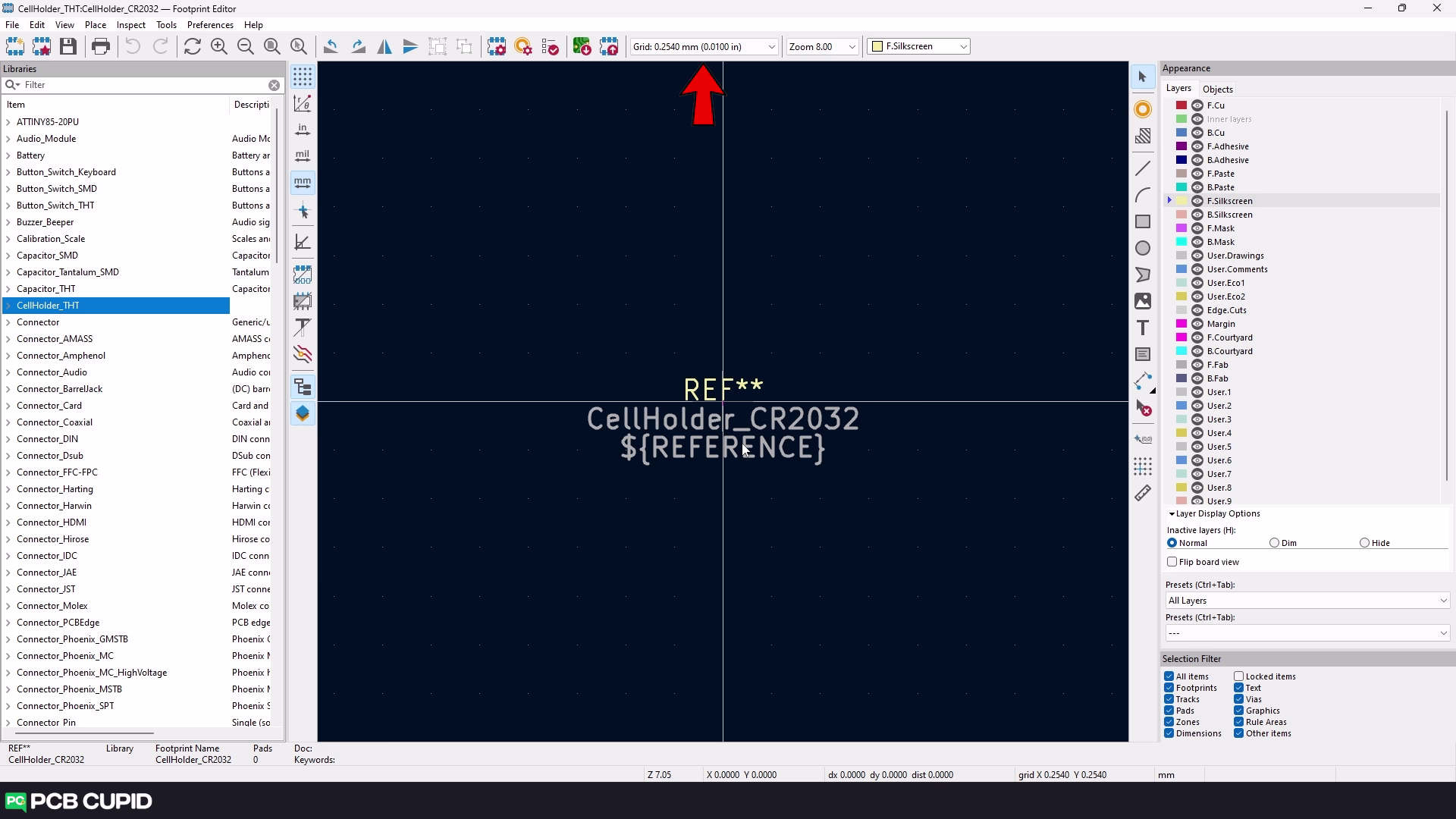
And the name of this footprint is “CellHolder_CR2032”.
Once the naming is done, select the through-hole option for the component. Since the component will pass through both layers of the PCB. With this, we have the library setup. Next, make sure you change the grid size to 10 mil to make the drawing more precise.
Creating Accurate Footprints in KiCad
Now with these settings, let’s try to draw the shape of the PCB with proper dimensions from the datasheet and start with the shape and size of the component.

So, make sure the silk layer is selected and select the circle tool. Draw a circle slightly larger than the diameter we need, so make the radius slightly larger than required. This will make the silk layer visible even after we solder the components. Once that’s done, we’ll go to the properties and change the thickness to 0.15 mm, which is recommended by the library convention.
Next, let’s add some pads so we can place the components on the footprint and solder them.
For this, you can use this pad tool and just click on the place where we need the pads to appear.

Kicad uses this pin information to associate the schematic symbol with the footprint during footprint assignment. So, make sure they have the same pin number. If you use pin 1 for a function on the symbol, make sure to use pin 1 on the footprint for the same function.
Now, to make the footprint accurate for the physical component, place the pads according to the measurements we have on the datasheet. If you want to make it more precise, you can also decrease the grid settings and use the measure tool.

There are quite a few things we need to make sure of while we create the footprint according to the library convention.
- Make sure the component is set to a through hole.
- Add the anchor to pin 1 of the footprint, we can do that by using this anchor tool and then clicking the first pad.
- Change the shape of the pin-1 to a rectangle
- Finally, make sure we have the solder mask checked for both layers.

These settings are not mandatory, but they will help us create a pretty good footprint with very minimal design errors.
Let’s also add some additional graphics to match the shape of the component.
Adding Custom Footprint in KiCad
To finish the footprint, we just have to add some courtyard to the footprint. We can do that by selecting the F copper layer and then drawing an outline around the component with a clearance of 10 mils.

To import this footprint into our project, just click on save. To verify, we can go to the PCB editor and click on preference, then click on manage footprint library. Here under Project, we can see the custom footprint we have created.

We can quickly replace the existing footprint to see how it affects our PCB. select the footprint, then right-click, and then click on Change Footprint.

Here, make sure the “footprint is selected” option is selected, then select the new footprint that we want to replace. To apply the change, click on Change. You can see that, after a few adjustments, we have successfully updated our custom footprint on the PCB.
External Footprints
Alternatively, we can also search for components online and then replace the footprint, especially if you are using sites like Mouser, where you can easily find the parts you would like to purchase. But if you shop anywhere else, you might end up using third-party sites like SnapEDA or Octopart.
Since we have already downloaded the part from SnapEDA in the previous video, we’ll just see how we can add that here. Click on this folder icon, navigate to the download folder, and select the folder where you have the kicad_mod file. We have Attiny85 because that’s what we previously downloaded.

Let’s try changing this footprint as well as see how it affects our PCB.

For better understanding you can watch the complete video tutorial here:
Until the next article keep learning and keep creating!
If you have any queries, please drop them here